As sprinters cross the finish line at the end of a 100-metre race, the winner is not always immediately clear; the event often ends in a photo finish and the viewers are unable to make out the exact order of the athletes, as they are simply moving too fast for the naked eye. However, their movements can be captured and temporally resolved using stroboscopic imaging. This principle is being used by physicists to image extremely quick processes in nanomaterials (pump-probe spectroscopy).
By Ute Schönfelder
Solution of quantum dots made of cadmium selenide.
Image: Jens Meyer (University of Jena)Dr Maria Wächtler and Dr Daniil Kartashov are running a research project within the collaborative research centre ›Nonlinear Optics down to Atomic Scales‹ (NOA CRC) to gain insights into the tiny structures that make up matter. The researchers are using nonlinear optical methods to study the basic building blocks of semiconductors, focusing not only on spatially resolving the atomic structures, but also on imaging the dynamic processes that happen inside them, such as the oscillations of charge carriers in atomic lattices which only last a few hundred femtoseconds.
In order to examine extremely fast processes in extremely small dimensions, two challenges have to be solved at the same time: »First of all, we need the right material for our investigation,« says Maria Wächtler. For this purpose, the chemist and her team are producing useful nanoscale semiconductors in their laboratory at the Leibniz Institute of Photonic Technology. »Secondly, we have to develop methods that are sensitive enough to detect interactions with such small structures while being able to image ultra-fast processes,« adds Daniil Kartashov, who works at the Institute of Optics and Quantum Electronics at the University of Jena as a specialist in time-resolved spectroscopic methods.
As part of their project, the researchers are examining different sizes, shapes and complexities of nanoscale semiconductor materials. The simplest objects are quantum dots: spherical lattices measuring only a few nanometres in size and consisting of a few hundred to a thousand atoms. »These are sometimes referred to as artificial atoms, because their electronic properties behave like single atoms,« explains Wächtler. Due to their low spatial dimensions, their charge carriers – the electrons – cannot move freely in the spheres and are fixed to very specific energy values, which means their properties are determined by quantum effects.
The quantum dots are made of cadmium selenide and measure between two and eight nanometres in diameter. To give you a rough idea of how small a nanometre is, it might help to draw a comparison: The difference between a nanometre (one millionth of a millimetre) and a metre is proportionally the same as the difference between the diameter of a one-penny piece and the diameter of the earth. Such structures are practically ›invisible‹ for linear optical methods.
From infrared radiation to visible light
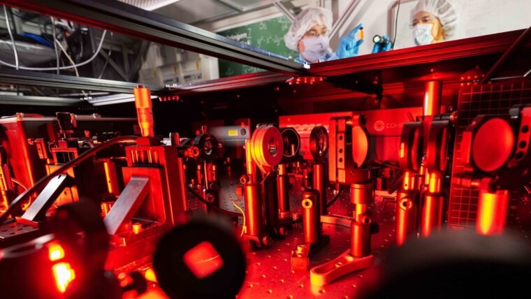
In order to learn how such nanoscale semiconductors work (e.g. how charges are transported in them and how vibrations are propagated within the atomic lattice), a novel, highly sensitive diagnostic method is required. For this purpose, Daniil Kartashov and his team of researchers are generating high harmonic optical oscillations. »These oscillations are caused by interactions between laser light and the examined material; their frequency is many times greater than that of the incident light,« says Kartashov. However, high harmonics can only be created if the incident light has a very high field strength. The laser used to excite the quantum dots has an output power of 300 billion watts per square centimetre. In order to prevent the material from immediately evaporating, the laser is pulsed so that the material is only exposed to the light for approximately 100 femtoseconds (100 millionths of a billionth of a second).
»This short period is enough for the laser light to interact with the electrons in the atomic lattices and generate high harmonics,« says Kartashov. The excitation laser emits pulses with a wavelength of approx. 4,800 nm in the mid-infrared spectrum, which are invisible to the human eye. The generated harmonics have wavelengths fractional to the laser wavelength: The 3rd harmonics measure 1,600 nm, the 5th harmonics measure 960 nm and so on. »We record the spectra of the rays generated between the 5th and 13th harmonics,« says Kartashov. As the signals are extremely weak, however, approximately 1,000 pulses a second are shot at the sample and the individual shots are accumulated.
This is how the researchers obtain initial snapshots from the material. Another laser beam enables the scientists to trigger the material’s inner dynamics before the laser pulses generating harmonics. This excitation laser sets the electrons and the lattice in motion, and then the second laser pulse comes with a variable delay to take snapshots of these dynamics. Recording spectra of the generated harmonics results in a series of images of the lattice dynamics which are similar to those found in sports photography, when very fast movements are resolved into individual images, such as a photo finish of sprinters crossing the finish line.
The researchers are applying this method, known as ›pump-probe spectroscopy‹, to various nanomaterials. In addition to quantum dots, they are investigating nanowires and also single-atomic-layer membranes produced by Prof. Turchanin and his team. »This provides information about how different structures and geometries affect the optical properties of semiconductor materials at nanoscale,« says Maria Wächtler, who explains that this area of research is still very much in its infancy but is already showing considerable potential for a range of practical applications. »This knowledge could enable us to develop photonic semiconductors for photonic computer chips,« says Kartashov. In contrast with electronic chips, the great advantage of photonic technology is that information could be processed at a significantly higher rate, as the speed of light is at least 1,000 times faster than the electron transport chain.
