Maximum surface area, minimum thickness: Research teams from materials science and physics are growing ultra-thin, inorganic materials consisting of only a single layer of atoms. In combination with nanoscale optical antennas, they are tailoring 2D materials to form photonic nanomaterials.
By Ute Schönfelder
Despite the fact that the crystals are less than one nanometre thick, they are incredibly robust. As they hardly have any volume, they are usually just referred to as ›2D materials‹. Similar to graphene, the first 2D material to be artificially produced, the ultrathin molybdenum or tungsten disulphide sheets have a number of extraordinary properties. »These ultimately thin semiconductor materials are suitable for various applications, such as new types of electronic and optoelectronic components, chemical sensor components and catalysts,« explains Andrey Turchanin.
Turchanin synthesizes the 2D materials in his laboratory by heating and evaporating the precursor materials at over 700°C. These materials are transported through a glass tube in a stream of argon and hydrogen gas at a defined pressure and temperature, which causes a reaction. The material crystallizes on a substrate within the tube, similar to the way in which water forms frostwork on a cold window pane. The ›ice crystals‹ made of tungsten disulphide are shaped like equilateral triangles (see picture below), while other 2D materials crystallize in the shape of stars or ›snowflakes‹.
Andrey Turchanin and his colleagues at the Institute of Physical Chemistry are producing 2D materials to develop ultrathin photonic structures with which to investigate nonlinear optical phenomena. The two-dimensional crystals are highly suitable for this, because of their symmetry-broken crystal structure, which is necessary for strong (so-called second-order) nonlinear optical effects to occur.
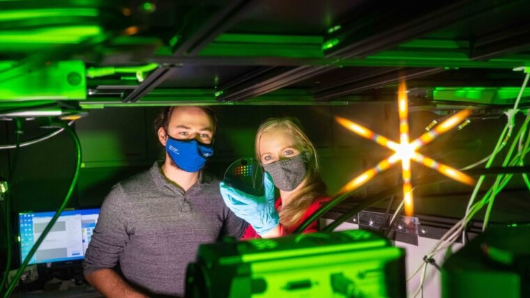
However, the 2D layers are so thin that they would be almost invisible to incident laser light, as they are much less thick than the wavelength of the light used. In order to enable the 2D material to interact efficiently with light, the researchers are therefore also equipping the membranes with tiny antennas that focus light in the near field to fall below the diffraction limit.
2D material combined with a silicon layer equipped with nano-antennas
This step is done in Prof. Dr Isabelle Staude’s laboratory. The nano-antennas are made as a thin layer using electron-beam lithography. In this process, custom shapes are drawn onto a mask by exposing a so-called ›resist‹ to a beam of electrons and the nanostructure is then transferred to the material (e.g. silicon) via an etching process. The nano-antennas created in this way measure between a few tens and a few hundreds of nanometres in size. When a layer of lithographed antennas is examined under an electron microscope, it looks like a piece of bubble wrap. »Both layers can be combined to create a hybrid system with optical properties that cannot be found in natural materials,« says Prof. Dr Isabelle Staude from the Institute of Solid-State Physics. In the future, the hybrid systems could be used as miniaturized sources of single or entagled light particles. This makes them suitable for applications in quantum technology, such as the encryption of optically transmitted information.
Nonlinear frequency doubling in nano-antennas
One of the nonlinear optical effects that can be produced and analysed with 2D membranes equipped with nano-antennas is nonlinear frequency doubling (see information box below). In this process, photons are generated that oscillate at twice the frequency of the incident light. Isabelle Staude explains the effect: »We expose the sample to laser pulses with a wavelength of 850 nm and, apart from the incident frequency, we also obtain laser light with a wavelength of 425 nm.« The light generated in this process is detected and analysed. The researchers are not only interested in the intensity of the radiation generated in this way, but above all in the light’s polarization properties. Polarization is one of the key properties of light and can be used, for example, to encode information. In naturally occurring materials such as phosphate or borate crystals, there is a fixed relationship between the polarization of the incident light and the laser light created; by contrast, the hybrid systems present completely new possibilities for tailoring the polarization properties of nonlinear light. That’s exactly what the researchers want to exploit.
Staude, Turchanin and their teams are conducting experiments to investigate how different geometric nanostructures influence the nonlinear optical effects; they are looking to design the nano-antennas in such a way that they can be used to control certain effects in a targeted manner. Another long-term goal is the production of optically switchable components. For this purpose, the 2D materials will be functionalized to enable them to react independently to changing ambient conditions such as light.
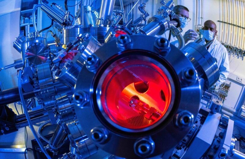
Prof. Dr Andrey Turchanin (left) and Dr Antony George are working on the "Ultra-High Vacuum (UHV) Multiprobe System" at the Institute of Physical Chemistry. The system enables more than ten different highly sensitive microscopic and spectroscopic methods for analysis of ultra-thin material samples. A high accuracy of measurements in the system, which was built especially for Prof. Turchanin and his team, is achieved by generating an ultra-high vacuum during measurements; when the machine is run-ning, there are fewer gas particles in the Multiprobe System than there are in the vacuum between the earth and moon.
Image: Jens Meyer (University of Jena)Nonlinear frequency doubling
When laser light interacts with a nonlinear material (e.g. a crystal with a certain non-centrosymmetric lattice structure), radiation is generated with twice the frequency of the incident light. When the frequency is doubled, the light’s wavelength is halved. In this way, for example, green light with a wavelength of 532 nm can be produced from the infrared radiation of an Nd:YAG laser with a wavelength of 1,064 nm. This phenomenon is used in laser pointers. The effect is caused by the oscillations of charge carriers in the crystal, which are produced through interactions with intense laser light.
As nonlinear frequency doubling is also referred to as ›second-harmonic generation‹, it is often abbreviated as SHG.
